


dual inline package Safety Certifications
A Dual Inline Package (DIP) is a type of electronic component package that features two parallel rows of electrical connecting pins. Ensuring the safety of these components is critical in protecting both the end users and ensuring compliance with regulatory standards.
Safety Certifications for DIP Components:
1. UL (Underwriters Laboratories):
– UL certification ensures that DIP components meet specific safety standards designed to minimize risks such as fire and electric shock. UL’s testing evaluates factors like performance under high-temperature conditions and the physical integrity of the packaging materials.
2. CE Marking (Conformité Européenne):
– A CE mark on DIP components indicates conformity with European safety, health, and environmental protection standards. It addresses risks related to electrical, mechanical, and thermal properties to ensure safe use within the European Economic Area.
3. RoHS (Restriction of Hazardous Substances Directive):
– RoHS certification ensures that DIP components do not contain specific hazardous substances like lead, mercury, and cadmium. This certification is crucial for reducing environmental and health risks associated with electronic waste.
4. CSA (Canadian Standards Association):
– The CSA certification demonstrates that DIP components meet Canadian standards for safety and performance. Like UL, CSA evaluates the materials and construction of the components to ensure they operate safely under expected conditions.
5. IEC (International Electrotechnical Commission):
– IEC standards encompass international benchmarks for safety and performance in electrical and electronic components, including DIPs. Compliance with IEC standards ensures that DIP components are globally recognized for their safety and reliability.
6. IPC-A-610:
– This standard outlines the acceptability of electronic assemblies, including DIP components, focusing on criteria for soldering, materials, and workmanship to ensure safe and reliable operation.
Manufacturers aiming to market their DIP components internationally should strive to achieve these certifications to guarantee broad compliance with safety regulations, thereby minimizing risks to users and ensuring broad acceptance in global markets.
List Reference Technical Parameters of “dual inline package”
A Dual Inline Package (DIP) is a type of electronic component package characterized by its rectangular housing with two parallel rows of electrical connecting pins. Here are the key technical parameters for DIP:
1. Pin Count:
– Commonly ranges from 4 to 64 pins.
– Pins are positioned on either side of the package.
2. Pin Spacing (Pitch):
– Standard spacing is typically 2.54 mm (0.1 inches) between adjacent pins in each row.
3. Package Dimensions:
– Widths vary, e.g., standard widths include 7.62 mm (300 mils) and 15.24 mm (600 mils).
– Length varies depending on the number of pins.
4. Pin Length:
– Standard pin length is approximately 3.1 mm to 3.8 mm for through-hole mounting.
5. Material:
– Package body is usually made of plastic (PDIP) or ceramic (CDIP).
6. Lead Configuration:
– Leads are either through-hole type, designed for soldering into a printed circuit board (PCB).
7. Package Types:
– PDIP (Plastic DIP), CDIP (Ceramic DIP), and SPDIP (Shrink Plastic DIP).
8. Thermal Resistance:
– Varies with material, typically around 20-50°C/W for plastic packages.
9. Power Dissipation:
– Influenced by package size and material, e.g., PDIP can dissipate up to 1-2 Watts without a heatsink.
10. Operating Temperature:
– Generally, the range is -40°C to +85°C for plastic DIPs and -55°C to +125°C for ceramic DIPs.
11. Mounting Style:
– Suitable for through-hole mounting techniques on PCB boards.
12. Electrical Parameters:
– Supported voltage and current ratings vary, specific to the IC housed within the DIP package.
By understanding these parameters, electrical engineers can effectively select and implement DIP-packaged components in their circuit designs, ensuring compatibility with PCB layouts and thermal management considerations.
List Product features of “dual inline package”
A Dual Inline Package (DIP) is a type of electronic component package used for integrated circuits (ICs). It is characterized by a rectangular housing with two parallel rows of electrical connecting pins. Below are the key product features of a DIP:
1. Pin Configuration: DIPs typically have a standard pin count ranging from 4 to 64 pins, arranged in two parallel rows. The pin spacing is usually 0.1 inches (2.54 mm).
2. Ease of Handling and Installation: The physical design of DIPs makes them relatively easy to handle, making manual assembly and prototyping straightforward.
3. Solderability: DIPs are designed for through-hole mounting on printed circuit boards (PCBs). The pins are long enough to penetrate through holes of a PCB for easy soldering on the opposite side.
4. Socket Compatibility: They can be inserted into DIP sockets, which allows for easy replacement, upgrading, and testing of ICs without additional soldering.
5. Thermal Performance: The through-hole design aids in better thermal dissipation compared to surface-mount devices (SMDs), helping to manage heat more effectively in some applications.
6. Mechanical Stability: The through-hole mounting method provides robust mechanical strength, ensuring that components are securely attached to the PCB, which is essential for high-reliability applications.
7. Versatility: DIPs can house a wide array of components, including microcontrollers, memory chips, and other digital or analog ICs. This versatility makes them suitable for various applications ranging from consumer electronics to industrial systems.
8. Cost-Effectiveness: Given their simplicity and ease of manufacturing, DIPs are often a cost-effective choice for many electronic applications, especially in environments where miniaturization is not a critical factor.
9. Identification: DIPs commonly come with clear labeling on the package, making it easy to identify the components during assembly and maintenance.
DIPs remain a popular choice in applications where ease of use, reliability, and mechanical strength are prioritized over miniaturization and advanced packaging technologies.
List Various Types of “dual inline package”
A Dual Inline Package (DIP) is a type of electronic component package with two parallel rows of pins designed for through-hole mounting on a circuit board. Here are various types of DIPs:
1. Standard DIP: The most common form, with pins spaced at a 0.1-inch (2.54 mm) interval. They range in size from 4 to 64 pins.
2. Skinny DIP (SDIP): Similar to standard DIPs but with a smaller body width. They typically measure around 7.62 mm, making them suitable for more compact designs.
3. Shrink DIP (Shrink Dual Inline Package, SDIP): Featuring a smaller pin pitch, usually 0.07 inch (1.778 mm), these packages save board space while accommodating more leads.
4. Ceramic DIP (CERDIP): Used for applications requiring high reliability and thermal performance. These are often utilized in aerospace and military sectors.
5. Plastic DIP (PDIP): The most widely used DIP type, made from plastic. It is commonly employed in consumer electronics.
6. Glass-Sealed Ceramic DIP: Offers enhanced reliability in high-stress environments, featuring glass-sealed lids for superior protection against moisture and contaminants.
7. Power DIP: Designed to dissipate more heat, these DIPs have broad leads to handle higher currents, often used in power electronics.
8. Flip-Chip DIP: This advanced type contains a flip-chip die mounted within a DIP configuration, allowing for better electrical performance and a smaller footprint.
These diverse DIP configurations cater to various applications, balancing factors like cost, thermal performance, size, and reliability.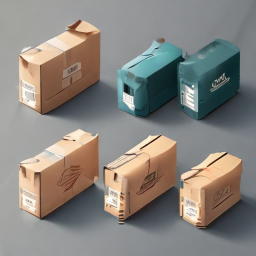
List Application of “dual inline package”
A Dual Inline Package (DIP) is a type of electronic component package with a rectangular housing and two parallel rows of electrical connecting pins. They are commonly used in:
1. Microprocessors and Microcontrollers: DIP packages are often used for housing microprocessors and microcontrollers due to their ease of handling and straightforward integration with other circuits. They are commonly seen in older PCs and embedded systems.
2. Memory Modules: Various types of memory chips, including RAM and EPROM, are frequently encapsulated in DIP packages. This is typical in retro gaming consoles, early computers, and other legacy systems.
3. Analog Devices: Operational amplifiers (op-amps), analog switches, and analog-to-digital converters often come in DIP packages. They are widely used in signal processing, sensor interfaces, and analog circuit design.
4. Power Management: Voltage regulators and some power controllers are available in DIP formats, making them accessible for use in power supply designs and battery-operated devices.
5. Interface ICs: DIP packages house a variety of interface chips, including UARTs, I/O expanders, and communication protocol converters. These are used in building communication interfaces in embedded systems and microcontroller projects.
6. Digital Logic Circuits: Various logic gates, counters, and other digital sequential and combinational logic circuits are frequently found in DIP packages. They are a staple in educational kits and prototype developments.
7. Consumer Electronics: Many early consumer electronic devices, such as appliances, calculators, and simple toys, utilized DIP components for their computing and control needs.
8. DIY Projects and Prototyping: The dual inline package is favored in hobbyist and educational settings because it’s easier to handle, test, and solder compared to surface-mounted devices (SMDs).
Despite the shift towards surface-mount technology (SMT), DIPs remain relevant for their reliability, ease of use, and simplicity in manual assembly.
List Buyer Types of “dual inline package”
The Dual Inline Package (DIP) is a popular type of packaging for electronic components, especially integrated circuits. Buyers of DIP components typically fall into several categories:
1. Electronics Hobbyists: These individuals often engage in DIY projects, working on custom circuits, and experimenting with electronics as a hobby. DIPs are popular in this group due to their ease of handling and soldering on breadboards or perfboards.
2. Educational Institutions: Schools, colleges, and universities often buy DIP components for their electronics labs. These institutions need these components for teaching purposes, allowing students to learn practical electronics and circuit design.
3. Prototype Developers: Engineers and designers building prototypes frequently use DIP components. They offer the flexibility to easily replace and modify circuits during the development stage, which is crucial for iterative design and testing.
4. Small and Medium Enterprises (SMEs): Smaller electronics companies often use DIP components for their product development and small-scale manufacturing. These businesses might not have the same resources as large corporations for surface-mount technology (SMT) and prefer the simplicity and cost-effectiveness of DIPs.
5. Repair Services: Technicians and repair services dealing with older or retro technology heavily rely on DIP components to replace faulty parts. Many legacy systems continue to use DIPs, making these components essential for maintenance and repair.
6. Legacy System Managers: Organizations that maintain older systems, such as certain industrial equipment, military technologies, and telecommunications infrastructure, often require DIP components to keep their systems operational.
7. Niche Market Manufacturers: Some manufacturers produce specialized electronics that still use DIP components, either due to specific design requirements or because their target application does not necessitate the move to newer packaging technologies.
Understanding these buyer types helps manufacturers and distributors tailor their marketing and sales strategies effectively, ensuring they meet the specific needs of diverse customer bases.
List “dual inline package” Project Types for Different Industries
Dual Inline Package (DIP) Project Types for Different Industries
1. Consumer Electronics:
– Microcontrollers and Microprocessors: Used in home appliances, toys, and personal gadgets for controlling operations and enabling smart functionalities.
– Memory Modules: Implemented in various consumer electronics for storage solutions.
2. Automotive:
– Engine Control Units (ECUs): Employed in vehicle control systems for optimal engine performance.
– Sensor Integration: DIPs serve as housings for various sensors used in adaptive cruise control, airbag systems, and tire pressure monitoring systems.
3. Medical Devices:
– Implantable Devices: Such as pacemakers and insulin pumps, where compact size and reliability are critical.
– Diagnostic Equipment: Used in portable diagnostic tools for point-of-care testing.
4. Industrial Automation:
– Programmable Logic Controllers (PLCs): Utilized in automation for manufacturing processes.
– Motor Control Systems: For driving motors in robotics and conveyor systems.
5. Telecommunications:
– Signal Processing Units: Used in modems, routers, and other communication devices for data processing.
– Power Management: Integrated into power supplies for telecommunications infrastructure.
6. Aerospace and Defense:
– Navigation Systems: Embedded in flight control and navigation units for aircraft and drones.
– Communication Systems: Used in secure communication and signal processing equipment.
7. Computing:
– Peripheral Interfaces: In keyboards, mice, and other input devices.
– Security Modules: For encryption and decryption functionalities within computing systems.
8. Renewable Energy:
– Inverter Circuits: For converting DC to AC in solar panel systems.
– Battery Management Systems (BMS): Ensuring efficient and safe energy storage and usage.
9. Wearable Technology:
– Fitness Trackers: Integration of DIPs in fitness monitoring devices for data processing.
– Smartwatches: Use of essential microcontrollers for applications and connectivity features.
DIPs serve a crucial role across various industries, providing reliable housing for essential electronic components that drive innovation and functionality.
dual inline package Accessories Upgrades and Custom Manufacturing Options
Dual Inline Package (DIP) is a widely utilized form for electronic components, particularly integrated circuits. To enhance their functionality and adaptability, several accessories, upgrades, and custom manufacturing options are available.
Accessories:
1. Sockets: Employing DIP sockets avoids direct soldering of ICs onto the PCB, facilitating easy replacement and reducing heat damage during soldering.
2. Heat Sinks: These accessories efficiently dissipate heat from high-power ICs, ensuring optimal performance and longevity.
3. Adapters: DIP to Surface Mount Device (SMD) adapters permit the use of DIP ICs in SMD circuits, providing enhanced flexibility.
Upgrades:
1. Gold-Plated Pins: Upgrading to gold-plated pins improves electrical connectivity and resistance to corrosion, especially in high-reliability applications.
2. Ceramic Packages: Switching from plastic to ceramic packages significantly enhances thermal and electrical performance, making them suitable for extreme environments.
3. Enhanced Pin Configurations: Customizable pin layouts can accommodate unique circuit designs, addressing specific engineering needs.
Custom Manufacturing Options:
1. Custom Pin Counts: Standard DIP ICs come in various pin counts, but custom manufacturing allows for tailored pin numbers to meet specific application requirements.
2. Specialized Materials: Utilize specialized materials like high-temperature plastics or ceramics to withstand specific environmental conditions or stringent industry standards.
3. Customized Marking: Custom labeling and branding ensure easy identification and add a professional aesthetic, which is critical for proprietary designs.
4. Enhanced Shielding: Advanced shielding techniques can be incorporated during manufacturing to protect against electromagnetic interference (EMI).
By leveraging these accessories, upgrades, and custom manufacturing options, DIP components can be optimized to meet a vast array of applications while improving the lifespan, reliability, and functionality of electronic devices.
List Quality Control and The Manufacturing Process of “dual inline package”
Manufacturing Process of Dual Inline Package (DIP)
1. Wafer Fabrication: The process begins with the creation of silicon wafers which serve as the base. Semiconductor circuits are built onto these wafers through photolithography, ion implantation, etching, and other steps.
2. Die Preparation: The wafer is sliced into individual dies, each containing a unique integrated circuit (IC). These dies are then cleaned and inspected for defects.
3. Die Attachment: Each die is attached to the lead frame using an adhesive or solder. The lead frame forms the ‘legs’ or pins of the DIP, facilitating electrical connections.
4. Wire Bonding: Ultra-fine wires (typically made of gold or aluminum) are bonded between the pads on the die and the pins of the lead frame, ensuring electrical connectivity.
5. Encapsulation: The assembly is encapsulated in a protective plastic or ceramic package to safeguard the IC from environmental damage. This is done via injection molding or transfer molding.
6. Trimming and Forming: Excess lead frame material is trimmed, and the pins are formed into the dual-inline shape, ensuring mechanical stability and ease of insertion into a socket or PCB.
7. Marking: Each package is marked with identification codes, part numbers, and manufacturing information, typically via laser marking or ink-jet printing.
8. Testing: Functional and parametric tests are conducted to ensure that each DIP meets specifications. This stage often involves automated testing equipment.
Quality Control in DIP Manufacturing
1. Incoming Material Inspection: Raw materials such as wafers, lead frames, and bonding wires are inspected for quality compliance upon arrival.
2. In-Process Checks: Continuous monitoring throughout each manufacturing stage, including die attachment, wire bonding, and encapsulation, helps identify and rectify defects immediately.
3. Automated Optical Inspection: Used for identifying visual defects and alignment issues post-die attachment and post-wire bonding.
4. Electrical Testing: Functional tests are conducted to ensure the IC performs as expected. Tests cover parameters like voltage, current, and signal integrity.
5. Burn-In Testing: Some DIPs undergo burn-in testing, where they are operated under elevated temperatures and voltages to identify early-life failures.
6. Final Inspection: A thorough visual and electrical inspection is performed on the final product to ensure it meets all quality standards before shipment.
How to use “dual inline package”
A Dual Inline Package (DIP) is a type of electronic component package characterized by its rectangular housing and two parallel rows of electrical connecting pins. DIPs are commonly used for integrated circuits (ICs), microcontrollers, and other semiconductor devices.
Steps to Use a DIP Component
1. Identify Pinout: Before using the DIP, obtain the datasheet for the component to identify the function of each pin (e.g., power, ground, input, output).
2. Prepare the Circuit Board:
– Breadboard: For prototyping, insert the DIP into the breadboard ensuring that pins go into separate rows.
– PCB (Printed Circuit Board): For a more permanent solution, align the DIP with the designated footprint and ensure the pin spacing matches the holes on the PCB.
3. Insert the DIP:
– Gently insert the DIP pins into the holes until the body is flush with the surface of the breadboard or PCB.
– If the pins are slightly bent, carefully straighten them with needle-nose pliers to avoid damage.
4. Connect Power and Ground:
– Refer to the datasheet and connect the power and ground pins to the corresponding sources on the breadboard or PCB. This step is crucial for the proper functioning of the component.
5. Wiring and Connectivity:
– Use jumper wires on a breadboard to make necessary connections to other components.
– For PCBs, solder the pins to secure the component and establish electrical connectivity.
6. Testing:
– Once everything is connected, power up the circuit and test the functionality using an oscilloscope or multimeter.
– Verify that the component operates as expected based on the intended application.
Tips:
– Handle the DIP carefully to avoid static discharge which can damage sensitive ICs.
– Double-check connections to ensure proper pin alignment and functionality.
– Use a chip puller for safe removal of the DIP from the socket if needed.
By following these steps, you can effectively integrate a DIP component into your electronic projects.
“dual inline package” Comparative Analysis
A Dual Inline Package (DIP) is a common type of electronic component package, characterized by two parallel rows of pins extending perpendicularly from a rectangular housing. This design facilitates easy insertion into a breadboard or a printed circuit board (PCB). Below is a comparative analysis of DIP in terms of its advantages, disadvantages, and alternative packaging types:
Advantages:
1. Ease of Handling: DIPs are conducive to manual handling, making them ideal for prototyping and small-scale production.
2. Versatility: They are compatible with both through-hole and socketed connections, allowing for flexibility during assembly and maintenance.
3. Reliability: Through-hole mounting provides strong mechanical bonds, reducing the risk of disconnection due to mechanical stress.
Disadvantages:
1. Space Consumption: DIPs take up more board space compared to surface-mount devices (SMD), which can be a limitation in compact or dense circuit designs.
2. Limitations in Pin Count: DIPs typically have fewer pins than other packaging types, limiting their use in high-density applications.
Comparative Alternatives:
1. Surface-Mount Device (SMD):
– Advantages: Smaller footprint, higher pin density, and better suited for automated manufacturing.
– Disadvantages: More challenging to manually solder and handle, requiring specialized equipment for assembly and repair.
2. Chip-On-Board (COB):
– Advantages: Even more compact than SMD, with direct mounting of the die onto the PCB, often resulting in lower costs.
– Disadvantages: Difficult to repair and requires sophisticated machinery for production.
3. Ball Grid Array (BGA):
– Advantages: High pin count and excellent electrical performance due to short lead lengths.
– Disadvantages: More difficult to inspect and repair. Requires advanced techniques for soldering and rework.
In summary, while DIPs offer ease of use and reliability for specific applications, their larger size and limited pin count present challenges in high-density and miniaturized designs. Alternatives like SMD, COB, and BGA address these limitations but come with their own sets of trade-offs, particularly in terms of ease of handling and repair.
“dual inline package” Warranty and Support
A Dual Inline Package (DIP) warranty and support typically cover several key aspects to ensure customer satisfaction and product reliability. The warranty period for DIPs can vary based on the manufacturer, but it often ranges from one to three years, starting from the date of purchase. During this period, the manufacturer guarantees that the DIP is free from defects in materials and workmanship under normal use. If a defect is found, the manufacturer will generally offer repair, replacement, or a refund, according to their specific policy.
To claim warranty support, customers are usually required to provide proof of purchase and a detailed description of the issue. Most manufacturers also have a return merchandise authorization (RMA) process to facilitate efficient handling of defective parts.
Support services typically include technical assistance through various channels such as phone, email, and online chat. Many manufacturers provide detailed datasheets, application notes, and frequently asked questions (FAQs) on their websites to help customers troubleshoot common issues. Online forums and community support groups can also be valuable resources.
For enhanced support, some manufacturers offer premium packages that include extended warranty periods, priority technical support, and access to exclusive resources. These packages may incur an additional cost but can be beneficial for critical applications requiring minimal downtime.
In summary, DIP warranty and support encompass a warranty period for defect-free products and robust customer support through multiple channels to ensure any issues are promptly addressed. Additional resources such as datasheets, application notes, and community forums supplement this support, providing a comprehensive safety net for DIP users.
List “dual inline package” FAQ
Dual Inline Package (DIP) FAQ
1. What is a Dual Inline Package (DIP)?
– A Dual Inline Package (DIP) is a type of electronic component package with two parallel rows of pins extending perpendicularly from a rectangular housing. It is used for mounting on a printed circuit board (PCB).
2. What are the common sizes of DIP?
– DIPs commonly come in widths of 7.62 mm (300 mils) or 15.24 mm (600 mils). The number of pins can vary, typically ranging from 4 to 64.
3. What materials are used in DIP construction?
– DIPs are usually made of plastic (PDIP) or ceramic (CDIP). The choice of material depends on the application, with ceramic offering better temperature and hermetic sealing properties.
4. How are DIP components mounted?
– DIP components are typically inserted into through-hole PCBs and soldered in place. They can also be used with sockets for easier replacement.
5. What are the advantages of using DIP?
– Ease of handling and assembly: The large size and spacing of pins make them easy to work with.
– Replacement and upgrade: Components can be easily swapped out if sockets are used.
– Availability: They are widely available and supported.
6. What are the disadvantages of using DIP?
– Board space: DIPs take up more PCB space compared to surface-mount devices (SMD).
– Performance limitations: They are less suitable for high-frequency applications due to larger inductance and capacitance.
7. Can DIP components be used for prototyping?
– Yes, DIP components are often used in breadboarding and prototyping due to their ease of insertion and removal.
8. Are there different types of DIP packages?
– Yes, there are various types such as PDIP (Plastic DIP), CDIP (Ceramic DIP), and SDIP (Shrink DIP).
9. What is the difference between DIP and SMD?
– DIP components are designed for through-hole mounting, whereas Surface Mount Devices (SMD) are designed for mounting directly onto the surface of PCBs.
10. What is a ZIF socket?
– A Zero Insertion Force (ZIF) socket is a type of socket used to connect DIP components to a PCB without applying force, thus minimizing the risk of damaging the pins.
This concise FAQ should offer a foundational understanding of Dual Inline Packages (DIP).
Top 10 FAQ with answer about dual inline package for Buyer Sourcing from China
Certainly! Here are the top 10 Frequently Asked Questions (FAQs) about buying Dual Inline Packages (DIPs) from China, with concise answers:
1. What Is a Dual Inline Package (DIP)?
A DIP is an electronic component package with two parallel rows of connecting pins. These are commonly used for microprocessors, switches, and other integrated circuits.
2. Why Source DIPs from China?
China is a major manufacturing hub offering competitive pricing, a wide range of suppliers, and the capability for both small and large-scale production.
3. How Do I Find Reliable Suppliers?
Use platforms like Alibaba, Global Sources, and Made-in-China. Look for suppliers with verified profiles, good reviews, and ample experience in the industry.
4. What Are the Quality Standards to Consider?
Ensure suppliers meet international standards such as ISO 9001 for quality management and RoHS for hazardous substance restrictions.
5. Can I Get Custom DIPs Made?
Yes, many Chinese manufacturers offer customization services. Provide your specifications and ensure the supplier has experience with custom orders.
6. What Are the Payment Terms?
Common terms include T/T (Telegraphic Transfer), L/C (Letter of Credit), and sometimes PayPal. Initial orders often require a deposit of 30-50%.
7. How Long Is the Lead Time?
Lead times vary but generally range from 2 to 8 weeks depending on the complexity and quantity of the order.
8. What Shipping Methods Are Available?
Options include air freight for speed, sea freight for cost-efficiency, and express services like DHL or FedEx for small quantities.
9. How Do I Ensure Product Authenticity?
Ask for samples, request testing reports, and consider third-party inspections. Use escrow services to hold payments until goods are verified.
10. What About After-Sales Support?
Confirm the supplier offers after-sales support, including warranties, return policies, and technical assistance. Clear communication channels are vital for resolving any issues.
These answers provide a foundational understanding for anyone interested in sourcing DIPs from China.